Advanced Chip Packaging Equipment Explained: Technologies, Processes, Applications and Benefits
Advanced chip packaging equipment plays an important role in modern semiconductor manufacturing. It refers to the specialized machines and systems used to connect, protect, align, and assemble semiconductor dies into packages that can be integrated into electronic products. As computing, artificial intelligence, automotive electronics, and telecommunications require greater processing capability, chip packaging has become an important part of semiconductor design and production.
Context
Advanced chip packaging equipment plays an important role in modern semiconductor manufacturing. It refers to the specialized machines and systems used to connect, protect, align, and assemble semiconductor dies into packages that can be integrated into electronic products. As computing, artificial intelligence, automotive electronics, and telecommunications require greater processing capability, chip packaging has become an important part of semiconductor design and production.
Traditional semiconductor manufacturing focuses heavily on creating electronic circuits on silicon wafers. After fabrication, individual dies must be separated, connected to electrical contacts, and protected within a package. Advanced packaging extends these methods by placing multiple dies or chiplets together, stacking components vertically, or connecting chips through very small electrical pathways.
What Is Advanced Chip Packaging Equipment?
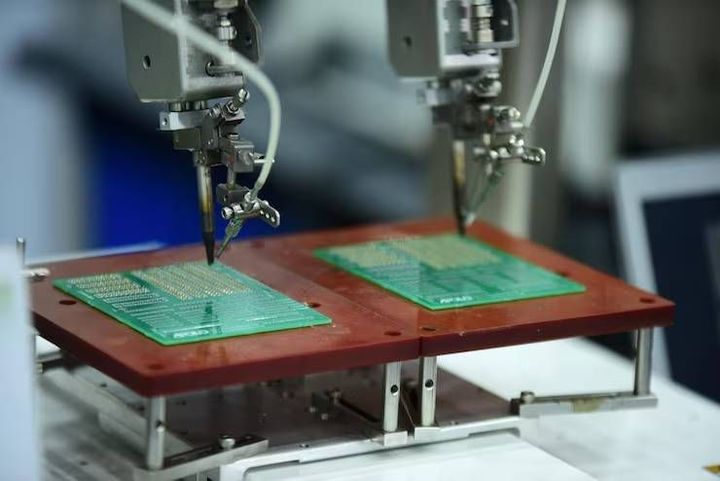
Advanced chip packaging equipment includes machines used during die placement, bonding, interconnection, encapsulation, inspection, and testing. These systems must handle delicate semiconductor components while maintaining precise alignment and controlling temperature, pressure, cleanliness, and material flow.
Common equipment categories include:
Die bonding machines: Position semiconductor dies on substrates or other dies.
Flip-chip bonding systems: Attach chips with electrical contacts facing downward toward a substrate.
Thermal compression bonding equipment: Uses controlled heat and pressure to form connections between components.
Wafer bonding systems: Join two wafers or wafer-level structures for particular packaging technologies.
Molding and encapsulation equipment: Applies protective materials around electronic components.
Inspection and metrology systems: Check alignment, dimensions, surface conditions, and possible defects.
The equipment selected depends on the package design, chip dimensions, interconnection method, production volume, and required reliability. Different packaging technologies can therefore require different combinations of machines.
Importance
Advanced chip packaging matters because shrinking transistor dimensions alone does not address every challenge in semiconductor performance. Modern processors and other complex devices may require multiple specialized chips to exchange data rapidly while managing heat, power consumption, and physical space.
Packaging technology helps manufacturers combine different semiconductor functions within a compact assembly. This approach is relevant to data centers, smartphones, automotive control systems, medical electronics, industrial automation, and communication infrastructure.
Major Applications of Advanced Packaging
One important application is high-performance computing. Artificial intelligence accelerators and graphics processors may combine processing dies with high-bandwidth memory, allowing large amounts of data to move between components within a compact package.
Automotive electronics also use sophisticated packaging for power management, sensing, control, and communication. In these applications, thermal behavior, vibration resistance, electrical insulation, and long-term reliability can be important design considerations.
Other applications include:
Consumer electronics: Compact processors, memory devices, and communication chips.
Telecommunications: Radio-frequency components and high-speed networking hardware.
Industrial equipment: Controllers, power electronics, sensors, and automation systems.
Aerospace and specialized electronics: Packages designed for demanding operating environments and specific reliability requirements.
Packaging Technologies and Their Equipment
Several technologies illustrate how packaging equipment supports different chip designs.
| Technology | Main purpose | Common equipment |
|---|---|---|
| Flip-chip packaging | Connect a die to a substrate through its contact bumps | Flip-chip bonders, reflow systems |
| Fan-out wafer-level packaging | Redistribute electrical connections beyond the original die area | Molding systems, redistribution-layer processing and inspection tools |
| 2.5D packaging | Place multiple dies alongside each other using an interposer or similar structure | Die bonders, interposer handling and bonding equipment |
| 3D stacking | Place dies vertically to shorten interconnections or increase integration | Precision bonders, wafer bonding and thinning equipment |
| Chiplet integration | Combine specialized dies within one package | Die placement, bonding and inspection systems |
These categories are related but not interchangeable. The design determines how dies communicate, how heat is removed, and which manufacturing steps are needed.
Recent Updates
From 2024 through 2026, advanced chip packaging has received increased attention as semiconductor manufacturers develop hardware for artificial intelligence, high-performance computing, and high-bandwidth memory. A notable industry direction is the integration of multiple chiplets within a single package rather than relying exclusively on one large silicon die.
This approach can allow different functions to be manufactured using different process technologies. However, it introduces challenges involving die alignment, interconnect density, thermal management, yield, and the testing of individual components before and after assembly.
Hybrid Bonding and Precision Assembly
Hybrid bonding connects components using direct metal-to-metal and dielectric-to-dielectric bonding, subject to the particular process design. It can support very fine interconnections compared with some conventional bump-based methods. Its implementation requires highly controlled surface preparation, cleanliness, alignment, and bonding conditions.
Equipment development in this area focuses on improving placement accuracy, wafer handling, surface inspection, and process control. Even small particles or surface irregularities can affect bonding quality, so cleanroom procedures and inspection are important parts of production.
Automation, Inspection, and Thermal Management
Advanced packaging production increasingly relies on automated material handling, machine vision, process monitoring, and data analysis. These technologies can help detect alignment problems, track production conditions, and identify variations between manufacturing stages.
Thermal management is another important area because densely integrated components can generate substantial heat. Package design and equipment processes must account for material properties, heat transfer, mechanical stress, and differences in thermal expansion. Progress varies by technology, manufacturer, and application, so individual equipment capabilities should be assessed against documented specifications.
Laws or Policies
Advanced chip packaging equipment is affected by semiconductor manufacturing regulations, workplace safety requirements, environmental rules, intellectual property protections, and international trade controls. The precise requirements depend on the equipment, materials, destination, end user, and manufacturing location.
Semiconductor Manufacturing Policy in India
India has developed semiconductor initiatives intended to expand domestic chip manufacturing, packaging, assembly, and testing capabilities. The India Semiconductor Mission supports the country's broader semiconductor development strategy, including the approved framework for semiconductor and display manufacturing projects.
The government's semiconductor programme has included support for semiconductor fabrication and assembly, testing, marking, and packaging activities under applicable scheme guidelines. Eligibility, financial support, approval conditions, and project obligations depend on the specific programme and its current rules.
Export Controls and Equipment Compliance
Some advanced semiconductor equipment, software, and related technologies may be subject to export controls. Requirements can depend on technical specifications, destination countries, end users, and intended uses. Businesses involved in cross-border equipment transactions must determine which licensing and documentation rules apply rather than assuming all machines are treated alike.
Manufacturing facilities must also follow applicable electrical safety, chemical handling, worker protection, waste management, and cleanroom requirements. Depending on the process, relevant controls may cover solvents, bonding materials, industrial gases, and equipment emissions.
Tools and Resources
Several technical resources help readers understand advanced chip packaging equipment, compare manufacturing approaches, and follow semiconductor industry developments. Technical documents are particularly important because similar machine names may describe different capabilities.
Industry and Technical Resources
SEMI publishes semiconductor manufacturing standards and industry information relevant to equipment, facilities, and manufacturing processes. IEEE publications provide technical research on semiconductor packaging, interconnections, thermal management, and electronic system integration.
The Semiconductor Industry Association publishes industry information and policy materials. India's Ministry of Electronics and Information Technology provides government announcements and information about semiconductor initiatives. These sources can help distinguish established requirements from proposed policies or industry forecasts.
Equipment Evaluation and Process Planning
Manufacturing teams may use equipment specification sheets, process-flow diagrams, defect-tracking templates, and production-capacity calculators to assess packaging operations. Useful comparison fields include:
Die and wafer dimensions supported by the machine.
Placement accuracy and bonding method.
Throughput under specified operating conditions.
Compatibility with substrates, materials, and package designs.
Inspection capability and defect-detection limits.
Maintenance requirements, facility conditions, and operator safety features.
A throughput estimate should account for loading, setup, inspection, rework, and downtime rather than relying only on a machine's maximum stated cycle rate. Actual production performance depends on the complete manufacturing line and process conditions.
FAQs
What is advanced chip packaging equipment used for?
It is used to align, attach, connect, protect, inspect, and test semiconductor dies during package assembly. The equipment supports technologies that integrate multiple chips or stack components vertically.
What is the difference between 2.5D and 3D chip packaging?
In 2.5D packaging, multiple dies are commonly arranged side by side on an interposer or comparable structure. In 3D packaging, dies or other components are stacked vertically, often to shorten connections or increase integration density.
Which machines are used in advanced semiconductor packaging?
Common systems include die bonders, flip-chip bonders, wafer bonders, thermal compression bonding machines, molding equipment, inspection tools, and testing systems. The exact combination depends on the package architecture.
Why is hybrid bonding important in advanced chip packaging?
Hybrid bonding can create very fine electrical connections between components while also bonding their surrounding dielectric surfaces. It requires precise alignment and careful surface preparation to achieve reliable connections.
How does India support semiconductor packaging?
India's semiconductor initiatives include policy frameworks intended to encourage domestic semiconductor manufacturing and packaging activities. Support depends on the relevant scheme, project eligibility, approval status, and applicable guidelines.
Conclusion
Advanced chip packaging equipment enables semiconductor manufacturers to assemble and connect increasingly complex electronic components. Technologies such as flip-chip packaging, chiplet integration, 2.5D packaging, 3D stacking, and hybrid bonding require different combinations of precision assembly, inspection, and process-control systems. Industry developments are shaped by computing demands, thermal challenges, manufacturing requirements, and government policies. Understanding these technologies and their equipment helps explain how modern semiconductor packages are produced and evaluated.