Semiconductor Lithography Machine Technology Explained: Types, Processes, Components and Applications
Semiconductor lithography machine technology is a central part of modern chip manufacturing. It involves transferring carefully designed patterns onto silicon wafers, which are thin discs used to produce integrated circuits. These patterns form the foundations of transistors, electrical connections, and other structures that allow electronic devices to process and store information.
Context
Semiconductor lithography machine technology is a central part of modern chip manufacturing. It involves transferring carefully designed patterns onto silicon wafers, which are thin discs used to produce integrated circuits. These patterns form the foundations of transistors, electrical connections, and other structures that allow electronic devices to process and store information.
The origins of semiconductor lithography are connected to traditional photographic techniques, in which light transfers a pattern onto a light-sensitive material. Chip manufacturers adapted this principle to create increasingly small and complex circuit structures. As electronic devices required greater computing power and energy efficiency, lithography systems developed to support finer patterns and more precise manufacturing processes.
What Is a Semiconductor Lithography Machine?
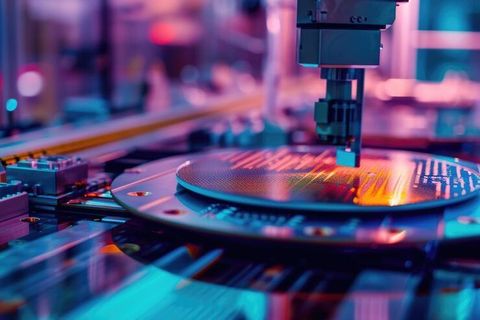
A semiconductor lithography machine uses a controlled light source, optical or reflective components, and a patterned mask or reticle to project circuit designs onto a wafer coated with a light-sensitive material called photoresist. The exposed photoresist changes its chemical properties, allowing selected areas to be removed during development.
Lithography does not create a complete chip in one step. It is repeated alongside processes such as deposition, etching, cleaning, and inspection to build multiple layers of structures on a wafer. The accuracy of each layer's placement is important because even small alignment errors can affect the operation of the finished circuit.
Why Lithography Matters in Chip Production
Semiconductor lithography determines many of the geometric features that can be formed during manufacturing. Its capabilities influence transistor density, circuit complexity, production requirements, and the range of chips a fabrication facility can manufacture.
Lithography is used in processors, memory chips, image sensors, communication components, and power-management devices. Different chip designs require different pattern sizes and manufacturing approaches, so semiconductor facilities may use several lithography technologies within the same production process.
Importance
Semiconductor lithography matters because electronic systems depend on integrated circuits with precisely defined structures. Smartphones, computers, vehicles, telecommunications equipment, medical instruments, industrial controllers, and data centers all use chips produced through semiconductor manufacturing processes.
The technology also presents practical challenges. Manufacturing facilities must maintain controlled environments, manage vibration and temperature, align successive circuit layers, and monitor defects. Lithography equipment is complex because it must coordinate optical systems, mechanical stages, chemical processes, and computerized controls with very high precision.
Main Challenges in Lithography
Several factors influence lithography performance:
Resolution: The ability to reproduce small circuit features on a wafer.
Overlay accuracy: How precisely a new pattern aligns with previously manufactured layers.
Throughput: The number of wafers or wafer exposures a system can process within a given period.
Defect control: The prevention and detection of unwanted particles, pattern errors, and surface irregularities.
Process stability: The ability to maintain consistent results across wafers and production runs.
Equipment integration: Coordination between lithography systems and other chip-manufacturing tools.
These factors are interconnected. Smaller patterns may require more demanding exposure conditions, while complex patterning approaches can involve additional processing steps and inspection requirements.
Types of Semiconductor Lithography Machines
Lithography systems are commonly classified by their exposure wavelength and patterning method.
| Technology | General characteristics | Typical applications |
|---|---|---|
| g-line and i-line optical lithography | Uses ultraviolet light at longer wavelengths than advanced deep-ultraviolet systems | Sensors, power devices, and other established processes |
| Deep ultraviolet (DUV) lithography | Uses wavelengths such as 248 nm or 193 nm | Logic, memory, and many other integrated circuits |
| Immersion DUV lithography | Uses a liquid between the final lens and wafer to improve optical resolution | Fine-pattern manufacturing and advanced multipatterning |
| Extreme ultraviolet (EUV) lithography | Uses light with a wavelength of about 13.5 nm and reflective optics | Selected advanced logic and other leading-edge production layers |
| Electron-beam lithography | Uses a focused electron beam to write patterns directly or through related techniques | Research, mask production, and specialized applications |
| Nanoimprint lithography | Transfers patterns using a physical template pressed into a suitable material | Selected specialized and emerging patterning applications |
The table describes broad categories rather than fixed limits. Actual capabilities depend on the system design, process conditions, materials, and manufacturing requirements.
Recent Updates
Semiconductor lithography continues to evolve as chipmakers develop advanced processors, memory technologies, and specialized integrated circuits. Developments from 2024 through 2026 have included broader industrial use of high-numerical-aperture EUV development platforms, continued refinement of conventional EUV systems, and efforts to improve patterning accuracy, equipment productivity, and process control. Adoption varies by manufacturer and production facility.
Extreme Ultraviolet and High-NA Lithography
EUV lithography uses light at approximately 13.5 nm. Because this light is absorbed by most materials, the system uses reflective optics rather than the conventional transparent lenses found in many optical systems. The light source, multilayer mirrors, vacuum environment, mask, and wafer-handling equipment must operate together under tightly controlled conditions.
High-numerical-aperture EUV systems use optical designs intended to resolve finer features than conventional EUV platforms. They introduce additional engineering demands, including mask considerations, resist performance, process integration, and equipment productivity. Industrial adoption is a gradual process involving evaluation, installation, qualification, and integration into manufacturing workflows.
Advances in DUV and Computational Lithography
DUV lithography remains important across a broad range of semiconductor manufacturing. Chipmakers use techniques such as multiple patterning to create structures that may be smaller than those produced in a single exposure. These approaches can increase the number of processing steps and place additional demands on alignment and defect control.
Computational lithography also plays a growing role in preparing patterns for manufacturing. Software models how light interacts with masks and photoresist, then helps adjust mask designs to compensate for optical effects. Process simulation, machine learning, and improved metrology tools can support defect analysis and manufacturing control, although results depend on model accuracy and production data.
Laws or Policies
Semiconductor lithography equipment is affected by trade controls, export regulations, intellectual-property protections, environmental requirements, and workplace safety rules. The relevant requirements depend on the equipment's technical specifications, the countries involved, the end user, and the intended application.
Semiconductor Equipment Export Controls
In the United States, export-control rules administered by the Bureau of Industry and Security can restrict certain advanced semiconductor equipment, related technology, and associated items destined for specified countries or end users. The scope of restrictions can change through regulatory updates, licensing requirements, and country-specific measures.
Other jurisdictions, including the Netherlands and Japan, also apply controls to certain semiconductor manufacturing equipment and technologies. These rules do not apply identically to every lithography machine. Classification, destination, technical capability, and end-use conditions determine which requirements may apply.
Manufacturing Standards and Environmental Requirements
Semiconductor facilities must also consider chemical handling, worker exposure, equipment safety, waste management, and energy use. Applicable requirements may include national workplace safety rules, environmental permits, electrical standards, and relevant international technical standards.
In India, semiconductor manufacturing and equipment-related activities may be affected by applicable factory legislation, environmental rules, import regulations, and government semiconductor initiatives. The India Semiconductor Mission supports the development of the country's semiconductor and display manufacturing ecosystem, subject to the relevant program conditions. Specific requirements depend on the project and the rules in force.
Tools and Resources
Technical publications, equipment documentation, simulation software, and semiconductor industry resources help readers understand lithography systems. The appropriate resource depends on whether the purpose is general learning, engineering analysis, equipment evaluation, or policy research.
Technical Learning and Industry Information
The following resources provide information about semiconductor technology and manufacturing:
ASML: Technical explanations of lithography principles, DUV systems, and EUV technology.
IEEE: Research papers and technical publications on semiconductor devices, lithography, and manufacturing methods.
SEMI: Industry information covering semiconductor manufacturing equipment, technical standards, and production practices.
imec: Research updates concerning advanced lithography, process integration, and semiconductor scaling.
NIST: Measurement science and technical resources relevant to precision manufacturing and semiconductor research.
These resources serve different audiences. Introductory articles are useful for learning terminology, while research papers and technical documentation provide deeper information about process limitations and engineering methods.
Simulation, Measurement, and Process Control
Computational lithography software can simulate optical exposure and help optimize mask patterns. Process-control systems track manufacturing conditions, while metrology equipment measures critical dimensions, layer alignment, and surface characteristics.
Common measurement concepts include critical dimension, overlay error, exposure dose, and defect density. These measurements help engineers determine whether a process remains within specified tolerances. The precise methods and acceptable ranges vary according to the chip design and manufacturing process.
FAQs
How does a semiconductor lithography machine work?
It projects a patterned image onto photoresist covering a silicon wafer. After exposure and development, selected regions remain or are removed, allowing subsequent etching or other processes to form circuit structures.
What are the main types of semiconductor lithography machines?
Major types include g-line and i-line optical systems, DUV systems, immersion DUV systems, EUV systems, electron-beam lithography equipment, and nanoimprint systems. Each uses a different method or operating wavelength and supports different manufacturing needs.
What is the difference between DUV and EUV lithography?
DUV uses deep-ultraviolet light, commonly at 248 nm or 193 nm, while EUV uses light at approximately 13.5 nm. EUV can form very fine patterns with fewer patterning exposures in some applications, but it requires specialized reflective optics and a vacuum environment.
What are the main components of a semiconductor lithography machine?
Major components include the light source, mask or reticle, optical system, wafer stage, alignment sensors, photoresist process interface, and computerized control systems. Their coordinated operation supports accurate pattern transfer.
What factors affect semiconductor lithography accuracy?
Important factors include optical resolution, focus, exposure dose, wafer movement, mask quality, resist characteristics, environmental stability, and alignment between layers. Equipment calibration and process monitoring help control these variables.
Conclusion
Semiconductor lithography machine technology transfers intricate circuit patterns onto silicon wafers and plays a central role in integrated circuit manufacturing. DUV, EUV, electron-beam, and other approaches support different patterning requirements, while optics, alignment systems, materials, and process controls influence accuracy. Recent developments focus on finer features, improved process integration, and manufacturing consistency. Export controls, safety requirements, and environmental regulations also shape how lithography equipment is developed, distributed, and used.

You May Also Like