Semiconductor Engineering Guide: Design Methods, Manufacturing Processes, Devices and Applications
Semiconductor engineering is the field concerned with designing, developing, producing, testing, and applying semiconductor devices. A semiconductor is a material whose electrical behavior can be controlled, allowing it to act as a switch, amplifier, sensor, or other electronic element. Silicon is widely used, while materials such as gallium nitride, silicon carbide, and gallium arsenide are used for particular applications.
Context
Semiconductor engineering is the field concerned with designing, developing, producing, testing, and applying semiconductor devices. A semiconductor is a material whose electrical behavior can be controlled, allowing it to act as a switch, amplifier, sensor, or other electronic element. Silicon is widely used, while materials such as gallium nitride, silicon carbide, and gallium arsenide are used for particular applications.
The modern semiconductor industry grew from advances in solid-state electronics and the integrated circuit. Instead of building electronic systems from many separate components, engineers learned to place large numbers of transistors and related elements on a small piece of material. This development created the foundation for computers, mobile devices, communication equipment, vehicles, industrial controllers, medical electronics, and many other technologies.
A semiconductor engineering guide usually covers several connected stages: design methods, wafer processing, device fabrication, packaging, testing, and application. Each stage affects how a chip behaves, how much power it uses, how reliably it works, and what type of system it can support.
How semiconductor devices work
A semiconductor device uses controlled electrical properties to manage current or signals. Transistors are central to modern chips because they can switch between electrical states and perform logical operations.
Integrated circuits combine many components on one semiconductor substrate. Depending on their design, they may contain processors, memory, power-management circuits, sensors, communication functions, or combinations of these elements.
Importance
Semiconductor engineering matters because electronic systems depend on chips for processing information, controlling energy, sensing physical conditions, and communicating data. A smartphone, vehicle, industrial machine, medical instrument, or data center may contain many different semiconductor devices.
The field also addresses practical engineering challenges. Designers must balance processing capability, energy use, heat generation, reliability, physical size, and manufacturing complexity. A chip intended for a vehicle may have different requirements from one designed for a mobile device or an industrial controller.
Where semiconductor devices are used
Common application areas include:
- Consumer electronics such as phones, computers, televisions, and household equipment
- Automotive systems for engine control, safety functions, charging, sensing, and driver assistance
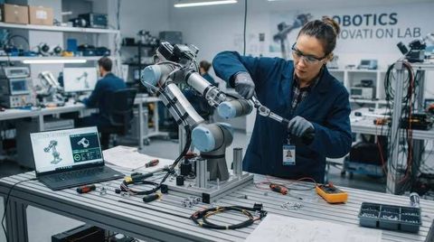
- Industrial automation for motor control, measurement, robotics, and monitoring
- Telecommunications for signal processing, networking, and wireless communication
- Healthcare equipment for imaging, monitoring, sensing, and laboratory systems
- Energy systems for power conversion, batteries, solar equipment, and electric mobility
- Computing and artificial intelligence for processors, memory, accelerators, and data processing
Main semiconductor engineering stages
| Stage | Main purpose | Typical output |
|---|---|---|
| Architecture | Define functions and system structure | Chip specification |
| Circuit design | Create electronic functions | Circuit design |
| Physical design | Arrange circuits on the chip | Layout |
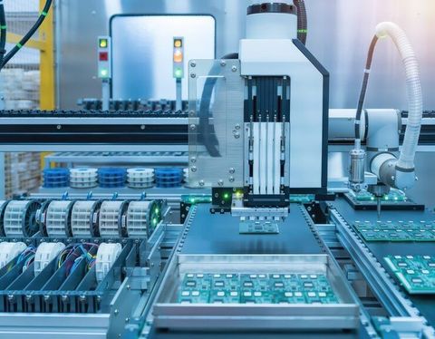
| Wafer fabrication | Form structures on semiconductor material | Processed wafers |
| Packaging | Protect and connect the die | Packaged device |
| Testing | Check electrical and physical behavior | Test results |
| Application | Integrate the device into a system | Working electronic system |
These stages are closely connected. A change in circuit design can affect manufacturing requirements, while packaging choices can influence heat transfer and electrical performance.
Recent Updates
Semiconductor engineering has been changing through greater demand for advanced computing, artificial intelligence, automotive electronics, power electronics, and connected devices. From 2024 through 2026, attention has also increased around domestic chip design, manufacturing capacity, advanced packaging, and supply-chain resilience.
Design and manufacturing trends
Chip development increasingly uses specialized processors and accelerators for particular workloads. Engineers are also working with chiplet-based architectures, where several smaller semiconductor dies can be combined within one package. This approach can separate functions and provide different design options for complex systems.
Advanced packaging has become an important part of semiconductor engineering. Techniques such as 2.5D and 3D integration can place multiple dies or layers closer together, which can improve communication between components while creating new requirements for heat management and testing.
Power semiconductor development is also expanding. Silicon carbide and gallium nitride are used in areas such as electric vehicles, charging equipment, renewable-energy systems, and power conversion because their material properties can support high-voltage or high-frequency operation in suitable designs.
In India, the India Semiconductor Mission has continued implementing programs for semiconductor fabs, compound semiconductors, packaging facilities, and chip design. The mission reported approvals and development activity across these areas during 2025, including semiconductor design initiatives.
Artificial intelligence and semiconductor design
Artificial intelligence workloads are increasing demand for processors that can perform large numbers of calculations efficiently. This is influencing chip architecture, memory design, interconnects, packaging, and thermal engineering. The result is a broader focus on complete system design rather than looking at the processor alone.
Laws or Policies
In India, semiconductor development is influenced by national programs administered through the Ministry of Electronics and Information Technology and the India Semiconductor Mission. The national semiconductor program includes schemes covering semiconductor fabs, display fabs, compound semiconductors, silicon photonics, sensors, discrete devices, assembly and packaging, and semiconductor design.
Design Linked Incentive
The Design Linked Incentive scheme is intended to strengthen semiconductor design in India. It covers areas such as integrated circuits, chipsets, systems on chip, systems, and intellectual-property cores, with financial support and design infrastructure provisions described by the India Semiconductor Mission.
Electronics Component Manufacturing Scheme
The Electronics Component Manufacturing Scheme was notified in 2025 to strengthen the electronics component ecosystem. Its covered areas include sub-assemblies, passive components, electro-mechanical components, printed circuit boards, selected circuit-board technologies, supply-chain components, and capital equipment used in electronics manufacturing. The scheme uses different incentive structures, including turnover-linked, capital-expenditure, and hybrid approaches.
These programs are part of a wider policy framework intended to deepen electronics manufacturing and semiconductor capabilities in India. Rules, eligibility conditions, application requirements, and support structures can change, so official government information is the appropriate reference for current policy details.
Tools and Resources
Semiconductor engineering involves specialized software, laboratory equipment, educational platforms, and reference materials. The tools used depend on whether the work involves architecture, circuit design, physical layout, fabrication, packaging, or testing.
Design and simulation tools
Electronic design automation tools can help engineers create circuit schematics, simulate electrical behavior, develop layouts, and verify designs before physical production. Semiconductor process simulation and device modeling tools can also help study how materials and structures behave under different electrical conditions.
Learning and reference resources
Useful resources include university electronics courses, semiconductor manufacturer documentation, technical standards, research papers, engineering textbooks, and government semiconductor portals. The India Semiconductor Mission also provides an introductory semiconductor learning platform designed for general audiences, covering basic concepts and real-world applications.
Common laboratory equipment
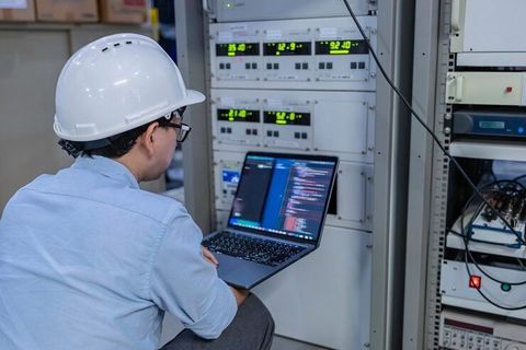
Depending on the stage of development, engineers may use oscilloscopes, semiconductor parameter analyzers, probe stations, thermal measurement equipment, microscopes, and reliability-testing systems. These tools help examine electrical characteristics, physical structures, heat behavior, and long-term device performance.
FAQs
What is semiconductor engineering?
Semiconductor engineering covers the design, fabrication, packaging, testing, and application of semiconductor devices. It combines concepts from electronics, materials science, physics, computer engineering, and manufacturing.
What are the main semiconductor manufacturing processes?
Common processes include wafer preparation, thin-film deposition, photolithography, etching, doping, cleaning, metallization, wafer testing, dicing, packaging, and final testing. The exact sequence depends on the device and manufacturing technology.
How are semiconductor devices designed?
Semiconductor device design begins with requirements and architecture, followed by circuit design, simulation, physical layout, verification, fabrication, packaging, and testing. Modern design methods use specialized electronic design automation tools throughout several stages.
What applications use semiconductor devices?
Semiconductor devices are used in computing, telecommunications, vehicles, industrial equipment, healthcare electronics, energy systems, consumer electronics, and many other electronic applications. Different devices are selected according to voltage, speed, power, sensing, processing, and environmental requirements.
Why is semiconductor engineering important in India?
Semiconductor engineering is relevant to India because national programs are supporting chip design, fabrication, packaging, component manufacturing, and related infrastructure. The India Semiconductor Mission coordinates several semiconductor and display programs as part of this broader ecosystem.
Conclusion
Semiconductor engineering connects chip design, materials, manufacturing, packaging, testing, and real-world electronic applications. Recent developments have increased attention on artificial intelligence hardware, advanced packaging, power semiconductors, and resilient supply chains. In India, government programs are supporting semiconductor design, manufacturing, packaging, and component development. Understanding these stages helps explain how small semiconductor devices become essential parts of modern electronic systems.